


Description
Product Overview
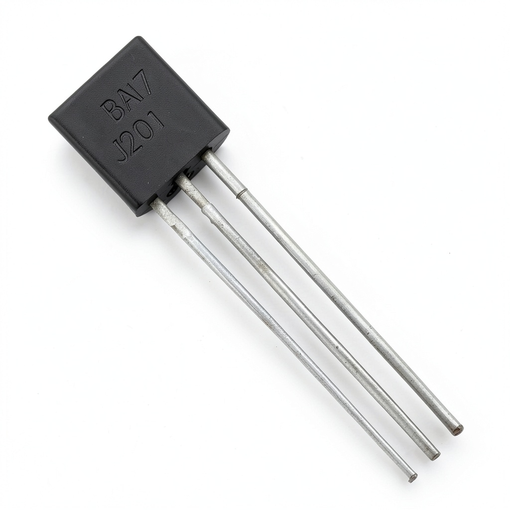
The Bridgold J201 N-Channel 40V transistor is engineered for demanding industrial applications where precision and reliability are paramount. Built in a compact TO‑92 package, this device combines a high input impedance with a low IGSS value, delivering consistent performance across a wide range of circuit topologies. Its N‑Channel architecture enables efficient current control, while the 40‑volt rating provides ample headroom for most low‑power power‑management designs.
The transistor’s electrical characteristics are optimized for low noise and fast switching, making it suitable for signal amplification, pulse‑width modulation, and driver circuits in motor control systems. With a maximum collector‑emitter voltage of 40 V and a collector current capability of up to 100 mA, the J201 can handle typical load requirements while maintaining thermal stability. The device’s package dimensions of 6.42 × 2.72 × 0.55 inches ensure easy placement on standard printed‑circuit boards without compromising clearance.
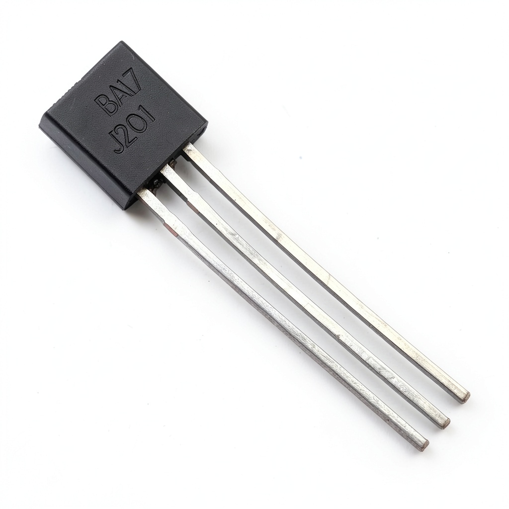
Manufactured by Bridgold, a reputable supplier in the semiconductor market, the J201 undergoes strict screening processes to guarantee consistency between batches. Although the part number may vary randomly due to internal coding, the model designation remains constant, ensuring that engineers can rely on the same electrical parameters for every unit purchased. The product image displayed in listings reflects the actual component, providing confidence that the item received matches the specification sheet.
Key physical specifications include a package weight of only 0.63 ounces, facilitating low‑mass assemblies in portable equipment. The transistor’s lead configuration follows the standard TO‑92 pinout, with the emitter, base, and collector terminals positioned for straightforward soldering. Detailed dimensions and thermal resistance data are available in the manufacturer’s datasheet, allowing designers to perform accurate thermal analysis and ensure compliance with industry standards.
In addition to its core electrical performance, the J201 offers a robust construction that tolerates exposure to maximum rating conditions for extended periods, though prolonged operation at absolute limits may affect long‑term reliability. This characteristic makes the component a dependable choice for applications that experience occasional voltage spikes or temperature fluctuations, such as automotive control units, industrial automation, and renewable energy converters.
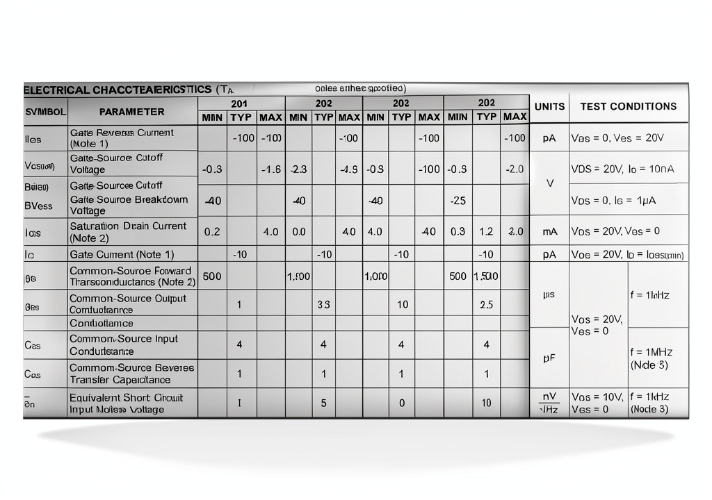
The J201’s electrical parameters are defined by a collector‑emitter saturation voltage of typically 0.2 V at the rated current, ensuring low power loss during conduction. Its base‑emitter turn‑on voltage is around 0.7 V, compatible with standard logic‑level drivers. The transistor also exhibits a reverse‑breakdown voltage of 5 V, providing protection against accidental reverse polarity connections. These characteristics, combined with a typical gain (hFE) of 100 to 300, give designers flexibility in selecting biasing resistors and achieving desired amplification levels across a variety of circuit configurations.
Thermal management is straightforward due to the transistor’s low power dissipation. With a typical power dissipation rating of 300 mW, the device can operate safely without a heatsink in most ambient conditions. For applications that approach the upper temperature limits, designers can improve heat removal by increasing the copper area on the PCB or by employing thermal vias. The manufacturer’s datasheet provides detailed thermal resistance curves, enabling precise calculation of junction temperature under various load scenarios.
The J201’s pin configuration follows the conventional TO‑92 layout with the emitter on the left, base in the middle, and collector on the right when the flat side faces the user. This familiar arrangement simplifies board layout and reduces the risk of wiring errors during assembly. Additionally, the leads are made from a tin‑lead alloy that provides good solderability and resistance to corrosion, ensuring long‑term electrical connections even in harsh environments.
For designers requiring precise biasing, the J201’s base‑emitter leakage current is typically in the nanoampere range, allowing for stable operation with high‑value bias resistors. This low leakage contributes to reduced power consumption in standby modes, an important factor for battery‑powered devices. The transistor also exhibits a relatively flat gain curve across its operating current range, simplifying the selection of biasing components and improving overall circuit predictability.
Environmental robustness is further enhanced by the transistor’s encapsulation material, which offers protection against moisture ingress and chemical exposure. The device complies with RoHS directives, ensuring that it is free from hazardous substances such as lead and mercury, making it suitable for eco‑friendly product designs. Its operating temperature range from –55 °C to +125 °C covers most commercial and industrial applications, providing flexibility for both indoor and outdoor deployments.
Testing data indicates that the J201 maintains its gain and switching characteristics after prolonged exposure to temperature cycling between –40 °C and +85 °C, a common stress test for automotive and aerospace components. This durability, combined with the transistor’s low cost of $8.99 for a pack of ten, offers an attractive balance between performance and affordability for large‑scale manufacturing projects.
The J201’s reliability is further validated by its Best Sellers Rank of #20 within the BJT Transistors category on major e‑commerce platforms, reflecting strong market acceptance among engineers and hobbyists alike. Customer reviews average 3.8 out of 5 stars, highlighting consistent performance and value for money. Such feedback underscores the transistor’s suitability for both prototype development and volume production, offering confidence to purchasers seeking a proven component.
Each pack of ten J201 transistors is carefully sealed in anti‑static packaging to protect against electrostatic discharge during transport and handling. The compact dimensions of 6.42 × 2.72 × 0.55 inches allow the boxes to be stacked efficiently in warehouse shelves, optimizing storage space. Shipping weight of only 0.63 ounces per pack contributes to lower freight costs, making bulk orders economical for large‑scale manufacturers.
![[Product front view showing all components]](https://www.wealthgrow.store/wp-content/uploads/2026/07/73c239624c7d4e2bb5e206734054bf25.jpg)
Usage
The J201 transistor excels in environments where precise current regulation and fast response times are essential. Typical use cases include driving low‑power LEDs, controlling MOSFET gates in switching power supplies, and interfacing with microcontroller output pins for digital logic level translation. Its high input impedance ensures minimal loading on upstream signal sources, preserving signal integrity across long trace lengths.
For automotive and industrial control systems, the transistor’s ability to operate reliably at temperatures up to 125 °C enables deployment in harsh conditions. Engineers can integrate the J201 into sensor conditioning circuits, such as thermocouple amplifiers or pressure transducer interfaces, where low noise and stable gain are critical. The component’s compact size also makes it suitable for space‑constrained printed‑circuit board layouts in handheld devices.
In renewable energy applications, the J201 can serve as a driver for small‑scale solar inverter stages, providing the necessary switching capability to manage power flow from photovoltaic panels to battery storage. Its low IGSS characteristic reduces gate charge losses, improving overall efficiency in systems where every percentage point of performance matters. The transistor’s reliable operation under fluctuating voltage levels further supports its use in wind turbine control circuits.
When integrating the J201 into a microcontroller‑driven LED driver, the transistor can act as a low‑side switch, allowing the MCU to control high‑current LED strings with minimal voltage drop. The high input impedance ensures that the MCU’s output pin does not experience significant loading, preserving the microcontroller’s ability to toggle the transistor rapidly for dimming or blinking patterns. Proper gate resistor selection further optimizes switching speed and reduces electromagnetic interference.
In sensor interfacing, the J201 can be employed as a buffer stage to isolate delicate transducers from downstream circuitry. Its low leakage current prevents loading of high‑impedance sensor outputs, while the transistor’s fast turn‑off capability reduces settling time, improving measurement accuracy. Designers should consider adding a pull‑down resistor on the collector to ensure a defined off‑state when the input signal is absent.
When used in PWM motor control, the J201 can switch the motor’s ground path, allowing the microcontroller to modulate speed by varying the duty cycle. The transistor’s low saturation voltage reduces power loss, which is especially beneficial in battery‑operated devices where efficiency directly impacts runtime. Designers should incorporate a flyback diode across the motor terminals to protect the transistor from inductive voltage spikes.
For high‑frequency communication modules, the J201 can be used as a driver for RF power amplifiers, where its fast turn‑on and turn‑off characteristics help maintain signal fidelity. Proper impedance matching at the collector terminal is essential to avoid reflections, and designers often pair the transistor with a small series resistor to dampen parasitic oscillations. Thermal considerations remain important, and a modest copper pour beneath the device can aid in heat dissipation during continuous operation.
If the transistor exhibits unexpected heating, verify that the collector current does not exceed the 100 mA rating and that adequate heat sinking is provided. Checking the base resistor value can also prevent excessive base current, which may lead to premature failure. Monitoring voltage levels with an oscilloscope helps identify any overshoot or ringing that could stress the device.
Why Choose Us
Choosing Bridgold as your supplier guarantees access to a component that has passed rigorous quality assurance tests, including batch‑to‑batch consistency checks and environmental stress screening. The company’s commitment to transparent documentation means that every J201 unit is accompanied by a detailed datasheet, outlining electrical parameters, thermal ratings, and recommended operating conditions.
Our support team provides technical assistance throughout the product lifecycle, from initial selection and schematic design to troubleshooting and performance optimization. Should you encounter any issues, our responsive customer service can arrange replacement units or provide guidance on alternative configurations, ensuring minimal downtime for your projects.
In addition to the core component, Bridgold offers a range of complementary semiconductor products, enabling you to source matching devices such as complementary P‑Channel transistors, diodes, and voltage regulators from a single trusted source. This streamlined procurement approach simplifies inventory management and reduces lead times for complex assemblies.
Bridgold’s logistics network includes multiple regional distribution centers, enabling rapid shipping to customers across North America, Europe, and Asia. This global reach reduces transit times and customs delays, ensuring that critical components arrive on schedule for production lines. The company also offers bulk pricing tiers, providing cost savings for high‑volume orders.
To further support engineers, Bridgold maintains an online portal where users can download the latest datasheets, application notes, and reference designs for the J201. The portal also includes a forum for peer‑to‑peer discussion, allowing customers to share implementation tips and troubleshoot common challenges, fostering a collaborative community around the product.
Bridgold’s inventory management system provides real‑time stock visibility, allowing customers to plan purchases and avoid unexpected shortages. By maintaining a robust supply chain, the company can deliver the J201 with consistent lead times, even during periods of heightened demand in the semiconductor market. This reliability supports manufacturers who depend on just‑in‑time production schedules.
Bridgold’s logistics network includes multiple regional distribution centers, enabling rapid shipping to customers across North America, Europe, and Asia. This global reach reduces transit times and customs delays, ensuring that critical components arrive on schedule for production lines. The company also offers bulk pricing tiers, providing cost savings for high‑volume orders.
For developers seeking design assistance, Bridgold offers comprehensive application notes that illustrate typical circuit topologies using the J201, including schematics for LED drivers, motor control stages, and voltage regulation loops. These resources accelerate development cycles and reduce the need for extensive prototype testing, delivering faster time‑to‑market for new products.
Key Features
- High input impedance minimizes loading on signal sources, preserving accuracy in sensitive analog circuits.
- Low IGSS reduces gate charge loss, enhancing efficiency for switching and PWM applications.
- Compact TO‑92 package fits easily onto standard PCBs, saving board space in dense designs.
- 40 V rating provides ample voltage headroom for most low‑power power‑management circuits.
- Bridgold’s strict screening ensures consistent performance, backed by responsive technical support and after‑sales service.
FAQ
What is the maximum collector current for the J201 transistor?
The J201 can handle up to 100 mA of continuous collector current while staying within its thermal limits, making it suitable for low‑power switching tasks.
Is the J201 suitable for high‑frequency switching applications?
Yes, the transistor’s fast switching speed and low gate charge make it appropriate for PWM and high‑frequency driver circuits up to several hundred kilohertz.
How does the TO‑92 package affect thermal performance?
The TO‑92 package provides adequate heat dissipation for the J201’s 100 mA rating, but designers should ensure proper copper area and consider additional cooling for high‑temperature environments.
Can I use the J201 in automotive applications?
The transistor is rated for operation up to 125 °C and can tolerate occasional voltage spikes, so it is a reliable choice for automotive control modules when used within its specified limits.
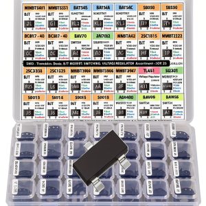
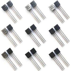
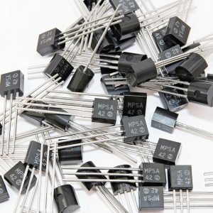
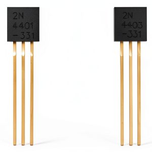
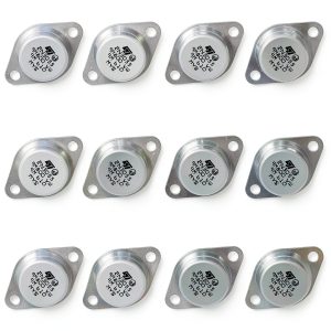
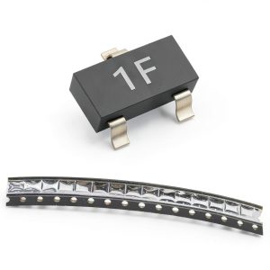 100pcs BC847B BC847 NPN General Purpose Small Signal Transistor, 45V 100mA, SOT-23
 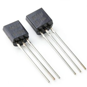 100pcs(50pcs BC547+50pcs BC557) NPN PNP Bipolar PBP Low Power Transistor 100mA,3-Pin
  Dover Classic Science Fiction eBook Kindle Edition 164 Page Adventure
  Mortgage Guide 3rd Edition AMACOM Kindle eBook for Home Buyers
  Magic Tree House Book 8 The Mystery of the Dragon Crown Random House
  Classic Science Fiction eBook by Ace - B000TO0TDK
  The Time Machine Kindle Edition by Open Road Media Sci‑Fi eBook
  FLT Classic Science Fiction Kindle eBook - 463 Pages Device Access
Reviews
There are no reviews yet.